
| +Home | Museum | Wanted | Specs | Previous | Next |

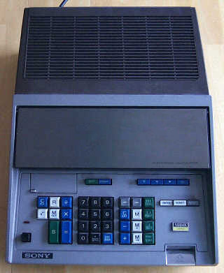
Sony SOBAX ICC-2550W Programmable Electronic Calculator
This wonderful machine is Sony's successor to its first programmable electronic desktop calculator, the ICC-2500, introduced in the winter of 1969. The ICC-2500 provided 111 steps of program storage and 7 memory registers and used a Sony-made magnetostrictive delay line for storing its working, memory, and program step data.
The ICC-2550 is the logical next step beyond the ICC-2500, but was still implemented using Sony's small-scale integrated circuit technology. The ICC-2550 offered mid-level functionality for the calculator buyer seeking a programmable calculator in the early 1970's. It provides the usual four functions plus square root, 253 step (over double that of the ICC-2500) programmability, nine memory registers, and importantly, offline program storage on magnetic cards, a feature missing from the earlier ICC-2500. The 2550 also provided a built-in printer interface (for Sony's EP-71 thermal printer), and of course, the high quality that classic Sony equipment was known for.
A view with the display cover in place
The SOBAX 2550 is very well-built, as was status-quo for Sony in those days. The base of the cabinet is a heavy plastic casting, and the upper half of the cabinet is a combination of plastic mated with a rather beefy aluminum casting that serves as the keyboard/display panel. The upper section of the case is removable by taking out two screws, sliding the upper section of the cabinet toward the rear of the machine slightly, and lifting it off. A removable hinged cover is provided that covers the display panel, providing both protection, and a more aesthetic look for the machine when it is not in use. The back panel of the machine has connections for the power cord, a switched auxilliary power outlet (for providing power to an external device, such as the optional printer), and a port for plugging in the external printer.

Profile view of the Sony Sobax 2550.
The ICC-2550, like it's predecessor, provides fifteen digits of capacity.
Fifteen digits is an unusual number for
the capacity of a calculator -- most machines use sixteen or fourteen.
The reason for this is that the machine actually calculates results to
17 digits, but the additional two digits are used for round-off
functions and improved accuracy. The display panel houses the fifteen
individual Nixie tube displays, along with 36 discrete
incandescent lamps for showing the status of programming functions, sign,
and error conditions. The calculator operates conventionally for calculators
of the time, with addition and subtraction working arithmetically, and
multiplication and division using algebraic entry, with the [=] key to
calculate the result for such operations. Decimal point location is fixed,
and set manually by using two keys
([◄∙] and [∙►])
that
move the decimal point to the left or right. The [CHG SIGN] key toggles
the sign of the number currently in the display, allowing the calculator
to properly handle mixed-sign operations. The 2550 has nine memory registers,
numbered 1 through 9, that can be stored into using the [M IN] key, recalled
from with [M OUT], and cleared using [M CLR]. The memory register to be
operated on is specified by a single digit keypress following the memory
function key. Memory registers can also be added to or subtracted from
by pressing the [M] key, followed by a memory register number, followed
by the [+] or [-] key. The [R] key swaps operands on the standard four
functions, for example:

The 2250 with the top part of the cabinet removed
The exhibited Sony ICC-2550W was built sometime in mid-1970 timeframe, based on date codes on components in the calculator. All but two of the 199 of the IC's that make up most of the logic of the 2550 are made by Sony, and are Sony-proprietary small-scale bipolar devices, with at most a few gates or a couple of flip-flops in each package. The logic supply for the Sony IC's is 4 volts, which makes it difficult to tell what type of logic is used. It definitely isn't conventional DTL(~4.5V) or TTL(5V) logic, as the supply voltage is too low, but it seems likely that the logic is similar in design to DTL or TTL. The Sony ICs are all 14-pin plastic dual-inline packaged (DIP) devices, with the +4V supply provided on pin 14, and Ground on pin 13. This arrangement of power supply pins being right next to each other is very unusual, and somewhat dangerous because during diagnostic testing a slip of a probe could accidentally short out the power supply. The spacing between the rows of pins on these Sony devices are slightly farther apart than that used by standard DIP packages. The reason that Sony opted for non-standard pin spacing is a mystery, as the Dual Inline package format had been standardized for quite some time by the time these devices were made, but it seems likely that Sony made the chips this way just because they were Sony. These devices are all Sony's 500-series logic, with only five different devices used in the machine, designated 501, 502, 503, 504, and 509. There appear to be two variations of the 501 device, with chips found with 501, and 501B designations. The same situation exists for the 502 device, with 502 and 502B devices found in the calculator. The 504 device was used in three different variations, with all of the 504 chips marked 504 in the usual location, but with some having an additional designation of 504-30 and 504-40. Some 504 chips have no additional designation on them. The circuit boards all carry designations next to the ICs, and the 504-30 and 504-40 designation appears on the circuit board in locations where these variations are used. The 503 and 509 chips have no variations as used in the ICC-2550.
It appears that this series of ICs was developed specifically for use in electronic calculators, and may have been the only use of these devices. There is no indication that Sony marketed the integrated circuits for sale outside the company.
Along with the Sony bipolar small-scale IC's, there are two PMOS medium-scale devices manufactured by National Semiconductor in the US. These devices are MM-5001 Dual 64-bit shift registers located on the delay line control board. The MM-5001 has two independent 64-bit shift registers, each with an input and output. Each shift register has two clock inputs, packaged in a TO-5 case with 12 pins. The clocking for each shift register requires two non-overlapping phases; an input phase that clocks the input stage of each of the 64 storage elements in the shift register on the falling edge of the input clock, and an output phase that copies the input stage of the each storage element into its output stage on the falling edge of the output clock. These shift registers can shift data through them at a rate of over 3 million shifts per second.
It isn't clear exactly what function these devices perform, but it seems feasable that the devices are used as the storage for the calculator's working registers, providing significantly faster access to the working registers than would be if the working registers were stored in the delay line. This architecture would substantially speed up general the general math operations of the calculator, as the solid state shift registers can operate at a signficantly faster shift rate than the delay line. If the working registers were stored in the delay line, the calculator logic would have to wait for the content of the memory registers and program step storage to circulate through it before it could access the working registers, which would slow the general operation of the calculator down significantly.
The calculator also uses a large number of discrete components, including
a significant number of diodes and resistors, as well as discrete transistors,
mostly used as logic gating where the Sony IC's did not have the type
of gating needed. A significant number of discrete components are used
used in the Nixie tube driving circuitry, where integrated circuit devices
simply weren't usable due to the high voltage switching required to drive
the Hitachi CD-80 Nixie tubes used.
The six circuit boards of the Sony Sobax 2550 (shown rear to front)
The electronics of the calculator are interconnected via a printed circuit board
backplane that also contains some circuitry related to keyboard
encoding and signal conditioning. The rest of the backplane board holds
edge-card connectors mounted at an angle to accept the six plug-in circuit
boards the contain the main logic of the calculator. The boards are mounted
at an angle to allow the cabinet to be significantly shorter (though
deeper as a result) than it would be if the board were mounted vertically.
Side View of Sony Sobax 2550 Internals
The card cage that
holds the plug-in boards is made of heavy cast and machined aluminum side
rails, and has stamped sheet-metal covers that shield the top and bottom
sides of the cage to minimize electromagnetic interference from
radiating out of the machine. The circuit cards are made of a
high-quality phenolic material, and have circuit traces on both sides
with plated-through holes to provide connections between the sides of
the board. The six boards are labeled A through F by etched characters
at the upper right hand corner of each board, with the A board
being the front-most Nixie display board, and the F board being the
rear-most delay line control board. One of the boards has high enough
density that there simply wasn't enough room for traces to make all of
the connections. This board has a number of jumper wires on the component
side of the board to provide the additional interconnections. Many of the
circuit boards also have hand-wired modifications made to them, such as
a diode or transistor tacked on to either side of the board. In general,
it is much less expensive to hand-add such engineering changes rather
than make circuit board design changes. Changes to circuit boards are
usually accumulated until a new production run is needed to meet
sales demand, then revisions were made to the circuit board artwork and
component layouts to incorporate the accumulated engineering changes.
The Delay Line Module
The rear-most (F) board in the card-cage
contains the circuitry for driving the magnetostrictive delay line that
serves as the working storage for the machine. This card has comparatively few
IC's on it, relying mostly on discrete components to shape, condition,
time, and drive the bits going into the delay line, along with providing
amplification, conditioning, re-timing, and level shifting for the bits
coming out. The delay line is mounted to the back-side of the controller
circuit card, and is about the same size as the circuit board.
The delay line used in the Sobax 2550 is very unusual in that it forms
the pulses in the delay line by contracting the delay line wire's length
then releasing it very quickly, generating a longitudinal pulse that travels
down the delay line to the other end. This is in contrast to the vast
majority of delay lines used in other electronic calculators, where the
wire is twisted to generate the pulse. This simplifies the design of
the delay line transducers, with a simple, but tiny solenoid (electromagnet)
in a spool around a point on the wire used to generate the magnetic
field needed to contract the magnetostrictive delay line wire by a miniscule
amount when current pulse flows through the coil of the electromagnet.
Assuming that the working registers of the calculator are stored
in the solid state MOS shift registers, and given that the 2550 has nine
memory registers and 253 steps of program storage, the delay line has
to store a fairly significant number of bits. Assuming a program step
consists of six binary bits (which makes for a nice even fit of
12 program steps in an 18-digit register, as well as allowing up to
64 unique program step codes), program step memory would consist
of 1,518 bits (6 bits per step X 253 steps). Assuming that each of the
nine memory registers consist of 18 digits (15 digits for display,
one guard digit, one digit for the sign of the number, and one digit
for the decimal point location), the memory registers would require 648 bits.
(18 digits per register X 4 bits per digit X 9 memory registers).
That would make for a total of 2,166 bits that would continually be circulating
through the delay line.
It is interesting to note that the delay line
has a label on it saying "UNREPAIRABLE! REPLACEMENT AT SONY SERVICE
CENTER ONLY". With as many bits as have to be crammed into the loop
of wire making up the delay line, the adjustments to the timing circuitry
to drive it must be critical, which could well explain why the delay line
was not deemed as not serviceable in the field.
A view of the back panel of the Sony ICC-2550W
The 2550 provides a reasonable set of
programming functionality. The green keys on the keyboard designate
the program functions. The operating mode of the calculator is set by two
keys that are mechanically linked so that only one can be depressed at any
time. These keys are labeled [MANUAL] and [AUTO]. When the machine is
in [MANUAL] mode, it acts like a regular calculator, with no programming
functions. When the mode is in [AUTO], then the calculator activates the
programming functions. Three more keys under a lid to protect them from
accidental activation control the programming mode of the machine.
Two of these keys are mechanically linked so that only one can be depressed
at any time, are [PROGRAM] and [CHECK]. When [PROGRAM] is depressed, and
the calculator is in "AUTO" mode, keypresses are stored in program memory.
This mode is used for entering programs. When [CHECK] is depressed, the
steps of the program can be verified step at a time, via indicators on the
display panel of the machine that light up for each key that is stored in
program memory. This mode can be used to debug programs. Last of the
three program mode keys is the [CORR] key, a momentary contact switch
that is used to allow program instructions to be edited by replacing a
program step with a different instruction. During program entry and
debugging, each step of the stored program is displayed via incandescent
indicators of the display panel of the machine. An indicator exists for
each key on the keyboard, and as each keycode in program memory is
encountered, the corresponding indicator lights up. This method of
indicating program steps is similar to that of the
Burroughs C3660 and Burroughs C3661.
Other green keys on the keyboard provide the ability to program
direct and indirect branches, conditional branches, and other programmed
functions such as marking the end of a program and control of the optional
external printer. Lastly, the green [S] key acts as a toggle for
starting/stopping execution of the program stored in memory.
The controls for the built-in
magnetic card reader/writer are located on the right-hand side of the
keyboard. A group of three keys, mechanically linked so that only
one can be depressed at any given time, control the mode of the card
reader, providing [ENTER], [VERIFY], and [RECORD] functions. The card
reader cycles by itself when a card is inserted in the slot at the
lower right edge of the keyboard, drawing the card in, then ejecting
it back out the way it came. When the [ENTER] key is depressed, the
program stored on the card is read into program memory. When in "VERIFY"
mode, the content of the card is compared with that in program memory,
and if a discrepancy is found, an ERROR condition is generated.
Lastly, when the card reader is in "RECORD" mode, the content of program memory
is written out to the card. The magnetic cards have Sony part number
MC-1000, and each card has one "side" for storage of program steps.
The 2550 does not have the capability of storing the memory registers
onto the magnetic card.


